We carry them everywhere, rely on them for everything, and panic the moment their screens go black. Modern smartphones are absolute marvels of engineering—housing billions of transistors, delicate sensors, and high-density logic boards within a frame just a few millimeters thick.
When a phone stops charging, drops into water, or refuses to boot up, most people see a mystery. But inside a modern repair lab, that mystery transforms into a systematic engineering process.
If you’ve ever wondered what actually happens behind the workbench, let’s step into the shoes of a beginner at Magnus Institute and trace the journey of a broken smartphone from initial diagnosis to a flawless repair.
The repair journey doesn't start with a screwdriver; it starts with systematic intake.
Before opening any device, a technician must establish a baseline:
Understanding logical intake prevents misdiagnosis and saves hours of unnecessary troubleshooting down the line.
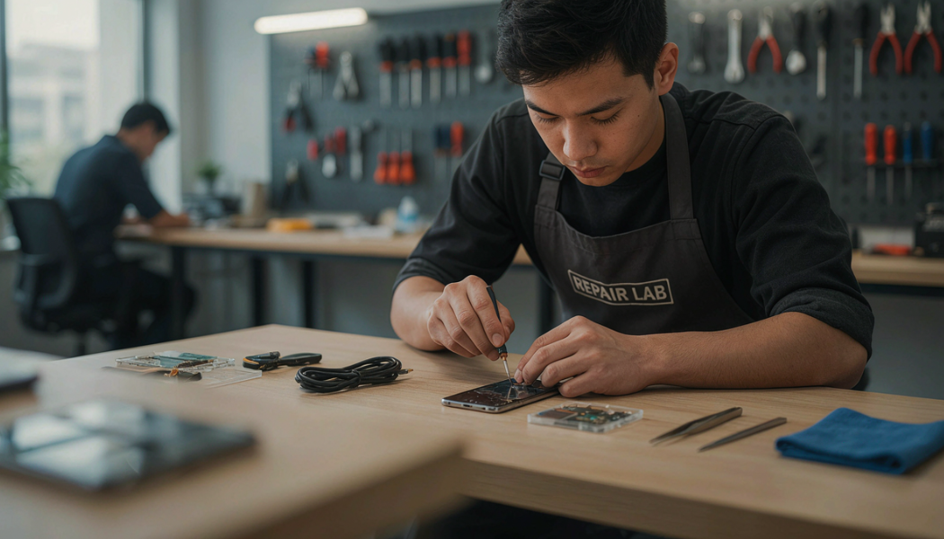
Step inside a professional lab like the ones at Magnus Institute, and the first thing you’ll notice is the emphasis on safety—for both the technician and the microchips.
Smartphones contain sensitive Integrated Circuits (ICs) that can be instantly destroyed by unseen Static Electricity. Before opening a device, technicians work on Electrostatic Discharge (ESD) safe mats, use grounded wrist straps, and work with specialized non-conductive pry tools (spudgers) to safely disconnect internal battery lines.
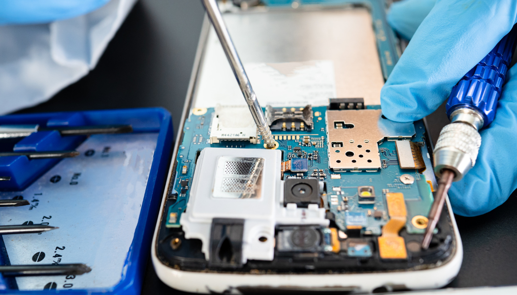
Opening a modern flagship device requires heat, precision, and patience.
Technicians use dedicated heat stations to soften water-resistant adhesives around glass back panels and displays. Once inside, the layout resembles a tiny, high-tech city:
A structured magnetic screw mat keeps every tiny screw in order—because putting a 1.4mm screw into a 1.2mm thread hole can cause permanent trace damage on the motherboard.
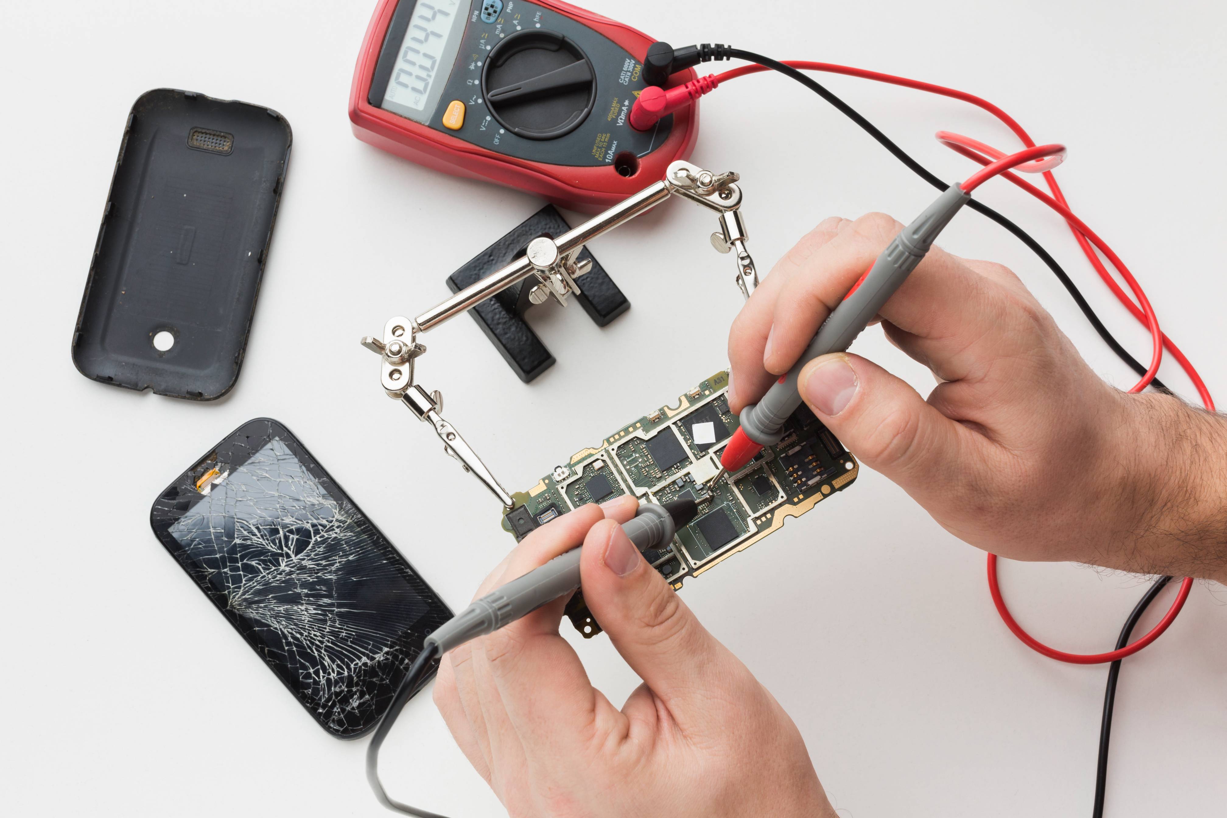
When the problem isn't as simple as a cracked screen or an aging battery, technicians step into deep troubleshooting:
This is where true engineering expertise comes to life. Basic repair shops stop at swapping modular parts, but advanced labs perform chip-level micro-soldering.
Under microscopic guidance, technicians use precision hot air rework stations and soldering irons fine enough to work on components smaller than a grain of rice:
Once the hardware issue is resolved, the device undergoes rigorous Quality Control (QC):
Only when all check-boxes are green is the smartphone sealed with fresh water-resistant adhesive and cleared for delivery.
Understanding what happens inside a repair lab is the first step toward mastering it. In an era where smartphone usage grows exponentially, skilled technicians who can perform precise, chip-level troubleshooting are in high demand worldwide.
At Magnus Institute of Technology, our TSSC-affiliated Smartphone Engineering programs take you from complete beginner to industry-certified expert. With state-of-the-art diagnostic equipment, hands-on micro-soldering labs, and 100% placement support, you don't just learn how to swap parts—you learn how devices work from the inside out.
Explore our Smartphone Engineering & Micro-Soldering Courses today at Magnus Institute!
 Magnus Forum